
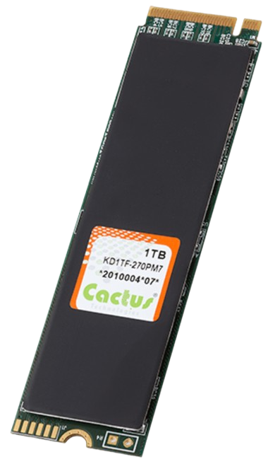
CACTUS Grade-270PM7 Series M.2 SSD
Introduction
In addition, it includes an on-drive intelligent controller that manages interface protocols, data storage and retrieval, as well as ECC, defect handling and diagnostics, power management, and clock control. The controller’s firmware is upgradeable, thus allowing feature enhancements and firmware updates while keeping the BOM stable.
Features
- Solid state design with no moving parts
- Capacities from 4GB to 256GB
- Compliant with Serial ATA 3.1 specifications
- ATA-8 ACS2 compatible
- Supports Serial ATA Generation I/II/III transfer rate of 1.5/3.0/6.0 Gbps
- Supports the ATA SMART Feature Set
- Supports the ATA Security Feature Set
- Supports Data Set Management (TRIM)
- Supports NCQ w/ max. queue depth of 32
- Supports DevSLP
- True Psuedo-SLC Mode
- ECC capable of correcting up to 66-bit errors per 1KB
- Enhanced error correction, < 1 error in 1014 bits read
- Voltage support: 3.3V±5%
Supported Standards
- ATA 8/ACS2 Specification published by ANSI
- Serial ATA 3.1 Specification published by the Serial ATA International Organization
Product Features
Cactus Technologies® Industrial pSLC mSATA SSD contains a high-level, intelligent controller. This intelligent controller provides many capabilities, including the following:
- Standard ATA register and command set (same as found on most magnetic disk drives).
- Manages details of erasing and programming flash memory independent of the host system
- Sophisticated defect management capabilities (similar to magnetic disk drives).
- Sophisticated system for error recovery using a powerful error correction code (ECC).
- Intelligent power management for low-power operation.
Host and Technology Independence
Cactus Technologies® Industrial pSLC mSATA SSD appears as a standard SATA disk drive to the host system. The drive utilizes a 512-byte sector, which is the same as that in an IDE magnetic disk drive. To write or read a sector (or multiple sectors), the host computer software simply issues an ATA Read or Write command to the drive as per the SATA protocol.
The host software then waits for the command to complete. Also, with the intelligent on-board controller, the host system software will not require changing as new flash memory evolves.
Thus, systems that support the Cactus Technologies® Industrial pSLC mSATA SSD products today will continue to work with future Cactus Technologies® Industrial pSLC mSATA SSDs built with new flash technology without having to update or change host software.
Defect and Error Management
Cactus Technologies® Industrial pSLC mSATA SSD contains a sophisticated defect and error management system similar to those found in magnetic disk drives. The defect management is completely transparent to the host and does not consume any user data space.
The soft error rate for Cactus Technologies® Industrial pSLC mSATA SSD is much lower than that of magnetic disk drives. In the extremely rare case where a read error does occur, the drive has sophisticated ECC to recover the data.
These defect and error management systems, coupled with the solid-state construction, give Cactus Technologies® Industrial pSLC mSATA SSDs unparalleled reliability.
Power Supply Requirements
Cactus Technologies® Industrial pSLC mSATA SSD operates at a voltage range of 3.3 volts ± 5%.
Product Specifications
For all the following specifications, values are defined at ambient temperature and nominal supply voltage unless otherwise stated.
System Environmental Specifications
| Cactus Technologies® Industrial pSLC mSATA SSD | ||
| Temperature | Operating: | 0° C to +70° C (Standard) -40° C to +85° C (Extended) |
| Humidity | Operating & Non-Operating: | 8% to 95%, non-condensing |
| Vibration | Operating & Non-Operating: | 20G, MIL-STD-883G Method 2005.2, Condition A |
| Shock | Operating & Non-Operating: | 3,000 G, MIL-STD-883G Method 2002.4, Condition C |
| Altitude (relative to sea level) | Operating & Non-Operating: | 100,000 feet maximum |
Power Requirements
| Cactus Technologies® Industrial pSLC mSATA SSD | ||
| DC Input Voltage (VCC) 100 mV max. ripple (p-p) | 3.3V ±5% | |
| (Maximum Average Value) See Notes. | Idle: Reading: Writing: | 100 mA 540 mA 660 mA |
Performance
| Read Transfer Rate | 4GB 8GB 16-256GB | Up to 150MBytes/sec Up to 300MBytes/sec Up to 540MBytes/sec |
| Write Transfer Rate | 4GB 8GB 16GB 32GB 64GB 128-256GB | Up to 70 MBytes/sec Up to 140 MBytes/sec Up to 275 Bytes/sec Up to 210 Mbytes/sec Up to 415 Mbytes/sec Up to 450 Mbytes/sec |
Reliability
| Data Reliability | < 1 non-recoverable error in 1014 bits READ |
| Endurance (estimated TBW): 4GB 8GB 16GB 32GB 64GB 128GB 256GB | Up to: 80TB 160TB 320TB 640TB 1280TB 2560TB 5120TB |
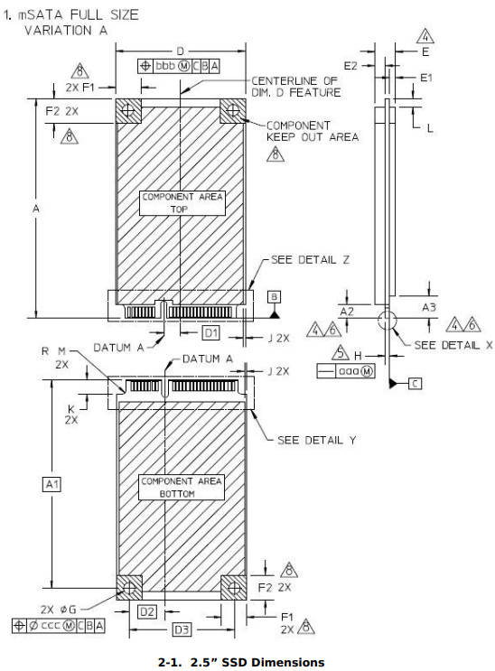
Physical Specifications
The following sections provide the physical specifications for Cactus Technologies® Industrial pSLC mSATA SSD products.
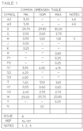
mSATA SSD Physical Specifications
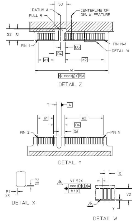
Interface Description
The following sections provide detailed information on the Cactus Technologies® Industrial pSLC mSATA SSD interface.
mSATA SSD Pin Assignments and Pin Type
The signal/pin assignments and descriptions are listed in Table 3-5.
mSATA SSD Pin Assignments and Pin Type
| Pin # | Pin Name | Description | Pin # | Pin Name | Description |
| 1 | Reserved | 2 | 3.3V | 3.3V supply | |
| 3 | Reserved | 4 | GND | ||
| 5 | Reserved | 6 | NC | Reserved for 1.5V supply | |
| 7 | Reserved | 8 | Reserved | ||
| 9 | GND | 10 | Reserved | ||
| 11 | Reserved | 12 | Reserved | ||
| 13 | Reserved | 14 | Reserved | ||
| 15 | GND | 16 | Reserved | ||
| 17 | Reserved | 18 | GND | ||
| 19 | Reserved | 20 | Reserved | ||
| 21 | GND | 22 | Reserved | ||
| 23 | RX+ | Host Receiver Differential Plus | 24 | 3.3V | 3.3V supply |
| 25 | RX- | Host Receiver Differential Minus | 26 | GND | |
| 27 | GND | 28 | NC | Reserved for 1.5V supply | |
| 29 | GND | 30 | I2C_CLK | Two-wire interface clock | |
| 31 | TX- | Host Transmitter Differential Minus | 32 | I2C_DAT | Two-wire interface data |
| 33 | TX+ | Host Transmitter Differential Plus | 34 | GND | |
| 35 | GND | 36 | Reserved | ||
| 37 | GND | 38 | Reserved | ||
| Pin # | Pin Name | Description | Pin # | Pin Name | Description |
| 39 | 3.3V | 3.3V supply | 40 | GND | |
| 41 | 3.3V | 3.3V supply | 42 | Reserved | |
| 43 | Device Type | No connection for mSATA | 44 | DEVSLP | DevSleep control |
| 45 | Vendor | Vendor-specific PIN | 46 | Reserved | |
| 47 | Vendor | Vendor-specific PIN | 48 | NC | Reserved for 1.5V supply |
| 49 | DAS/DSS | Device Activity signal | 50 | GND | |
| 51 | Presence Detect | Tied to GND in the device | 52 | 3.3V | 3.3V supply |
Electrical Specifications
The following table defines all D.C. Characteristics for the mSATA SSD products. Unless otherwise stated, conditions are:
- Vcc = 3.3V ± 5%
- Ta = -40°C to 85°C
Absolute Maximum Ratings
| Parameter | Symbol | MIN | MAX | Units |
| Storage Temperature | Ts | -55 | +100 | oC |
| Operating Temperature | TA | -40 | +85 | oC |
DC Characteristics
| Parameter | Symbol | MIN | MAX | Units |
| Input Voltage | Vin | -0.5 | Vcc + 0.5 | V |
| Output Voltage | Vout | -0.3 | Vcc + 0.3 | V |
| Input Leakage Current | ILI | -10 | 10 | uA |
| Output Leakage Current | ILO | -10 | 10 | uA |
| Input/Output Capacitance | CI/Co | 10 | pF | |
| Operating Current Idle Active | ICC | 105 665 | mA |
AC Characteristics
Cactus Technologies® mSATA SSD products conform to all AC timing requirements as specified in the SATA-IO specifications. Please refer to that document for details of AC timing for all operation modes of the device.
ATA Drive Register Set Definition and Protocol
The communication to or from the SSD is done using FIS. Legacy ATA protocol is supported by using the legacy mode defined in the SATA specifications. In this mode, the FIS has defined fields that provide all the necessary ATA task file registers for control and status information. The Serial ATA interface does not support Primary/Secondary or Master/Slave configurations. Each SATA channel supports only one SATA device, with the register selection as defined by the ATA standard.
ATA Task File Definitions
The following sections discuss the usage of the ATA task file registers. Note that the Alternate Status Register of legacy ATA is not defined for SATA drives.
Data Register
The Data Register is a 16-bit register, and it is used to transfer data blocks between the SSD data buffer and the Host.
Error Register
This register contains additional information about the source of an error when an error is indicated in bit 0 of the Status register. The bits are defined as follows:
| D7 | D6 | D5 | D4 | D3 | D2 | D1 | D0 |
| BBK | UNC | 0 | IDNF | 0 | ABRT | 0 | AMNF |
- Bit 7 (BBK) This bit is set when a Bad Block is detected.
- Bit 6 (UNC) This bit is set when an Uncorrectable Error is encountered.
- Bit 5 This bit is 0.
- Bit 4 (IDNF) The requested sector ID is in error or cannot be found.
- Bit 3 This bit is 0.
- Bit 2 (Abort) This bit is set if the command has been aborted because of a status condition: (Not Ready, Write Fault, etc.) or when an invalid command has been issued.
- Bit 1 This bit is 0.
- Bit 0 (AMNF) This bit is set in case of a general error.
Feature Register
This register provides information regarding features of the SSD that the host can utilize.
Sector Count Register
This register contains the number of sectors of CACTUS Grade-270PM7 Series M.2 SSD data requested to be transferred on a read or write operation between the host and the SSD.
Sector Number (LBA 7-0) Register
This register contains the starting sector number or bits 7-0 of the Logical Block Address (LBA) for any SSD data access for the subsequent command.
Cylinder Low (LBA 15-8) Register
This register contains the low-order 8 bits of the starting cylinder address or bits 15-8 of the Logical Block Address.
Cylinder High (LBA 23-16) Register
This register contains the high-order bits of the starting cylinder address or bits 23-16 of the Logical Block Address.
Drive/Head (LBA 27-24) Register
The Drive/Head register is used to select the drive and head. It is also used to select LBA addressing instead of cylinder/head/sector addressing. The bits are defined as follows:
| D7 | D6 | D5 | D4 | D3 | D2 | D1 | D0 |
| 1 | LBA | 1 | DRV | HS3 | HS2 | HS1 | HS0 |
- Bit 7 This bit is set to 1.
- Bit 6 LBA is a flag to select either Cylinder/Head/Sector (CHS) or Logical Block Address Mode (LBA).
- LBA07-LBA00: Sector Number Register D7-D0.
- LBA15-LBA08: Cylinder Low Register D7-D0.
- LBA23-LBA16: Cylinder High Register D7-D0.
- LBA27-LBA24: Drive/Head Register bits HS3-HS0.
- Bit 5 This bit is set to 1.
- Bit 4 (DRV): DRV is the drive number. This should always be set to 0.
- Bit 3 (HS3) When operating in the Cylinder, Head, Sector mode, this is bit 3 of the head number. It is Bit 27 in the Logical Block Address mode.
- Bit 2 (HS2) When operating in the Cylinder, Head, Sector mode, this is bit 2 of the head number. It is Bit 26 in the Logical Block Address mode.
- Bit 1 (HS1) When operating in the Cylinder, Head, Sector mode, this is bit 1 of the head number. It is Bit 25 in the Logical Block Address mode.
- Bit 0 (HS0) When operating in the Cylinder, Head, Sector mode, this is bit 0 of the head number. It is Bit 24 in the Logical Block Address mode.
Status Registers
These registers return the status when read by the host. Reading the Status register does clear a pending interrupt, while reading the Auxiliary Status register does not. The meaning of the status bits is described as follows:
| D7 | D6 | D5 | D4 | D3 | D2 | D1 | D0 |
| BUSY | RDY | DWF | DSC | DRQ | CORR | 0 | ERR |
- Bit 7 (BUSY) The busy bit is set when the device has access to the command buffer and registers, and the host is locked out from accessing the command register and buffer. No other bits in this register are valid when this bit is set to a 1.
- Bit 6 (RDY) RDY indicates whether the device is capable of performing operations requested by the host. This bit is cleared at power up and remains CACTUS Grade-270PM7 Series M.2 SSD cleared until the device is ready to accept a command.
- Bit 5 (DWF) This bit, if set, indicates a write fault has occurred.
- Bit 4 (DSC) This bit is set when the device is ready.
- Bit 3 (DRQ) The Data Request is set when the CACTUS Grade-270PM7 Series M.2 SSD device requires that information be transferred either to or from the host through the Data register.
- Bit 2 (CORR) This bit is set when a Correctable data error has been encountered and the data has been corrected. This condition does not terminate a multi-sector read operation.
- Bit 1 (IDX) This bit is always set to 0.
- Bit 0 (ERR) This bit is set when the previous command has ended in some type of error. The bits in the Error register contain additional information describing the error.
Device Control Register
This register is used to control the drive interrupt request and to issue an ATA soft reset to the drive. The bits are defined as follows:
| D7 | D6 | D5 | D4 | D3 | D2 | D1 | D0 |
| HOB | X | X | X | 1 | SW Rst | -IEn | 0 |
- Bit 7: This bit is used in 48-bit addressing mode. When cleared, the host can read the most recently written values of the Sector Count, Drive/Head, and LBA registers. When set, the host will read previously written values of these registers. A write to any Command block register will clear this bit.
- Bit 6 This bit is an X (Do not care).
- Bit 5 This bit is an X (Do not care).
- Bit 4 This bit is an X (Do not care).
- Bit 3 This bit is ignored by the drive.
- Bit 2 (SW Rst)This bit is set to 1 in order to force the drive to perform an AT Disk controller Soft Reset operation. The drive remains in Reset until this bit is reset to ‘0’.
- Bit 1 (-IEn) The Interrupt Enable bit enables interrupts when the bit is 0. When the bit is 1, interrupts from the drive are disabled. This bit is set to 0 at power-on and Reset.
- Bit 0 This bit is ignored by the drive.
Drive Address Register
This register is provided for compatibility with the AT disk drive interface. It is recommended that this register not be mapped into the host’s I/O space because of potential conflicts on Bit 7. The bits are defined as follows:
| D7 | D6 | D5 | D4 | D3 | D2 | D1 | D0 |
| X | -WTG | -HS3 | -HS2 | -HS1 | -HS0 | -nDS1 | -nDS0 |
- Bit 7 This bit is unknown. Implementation Note: Conflicts CACTUS Grade-270PM7 Series M.2 SSD may occur on the host data bus when this bit is provided by a Floppy Disk Controller operating at the same addresses as the SSD. The following are some possible solutions to this problem:
- Locate the SSD at a non-conflicting address (i.e., Secondary address (377) when a Floppy Disk Controller is located at the Primary addresses).
- Do not install a Floppy and an SSD in the system at the same time.
- Implement a socket adapter that can be programmed to (conditionally) tri-state D7 of I/0 address 3F7/377 when a SSD product is installed and conversely to tri-state D6-D0 of I/O address 3F7/377 when a floppy controller is installed.
- Bit 6 (-WTG) This bit is 0 when a write operation is in progress;s, otherwise, it is 1.
- Bit 5 (-HS3) This bit is the negation of bit 3 in the Drive/Head register.
- Bit 4 (-HS2) This bit is the negation of bit 2 in the CACTUS Grade-270PM7 Series M.2 SSD Drive/Head register.
- Bit 3 (-HS1) This bit is the negation of bit 1 in the Drive/Head register.
- Bit 2 (-HS0) This bit is the negation of bit 0 in the Drive/Head register.
- Bit 1 (-nDS1) This bit is 0 when drive 1 is active and selected.
- Bit 0 (-nDS0) This bit is 0 when the drive 0 is active and selected.
Command Description
- This section defines the ATA command set supported by Cactus Technologies® mSATA SSDs.
ATA Command Set
- Table 5-6 summarizes the supported ATA command set.
| COMMAND | Code |
| Check Power Mode | E5h, 98h |
| Data Set Management | 06h |
| Execute Drive Diagnostic | 90h |
| COMMAND | Code |
| Flush Cache | E7h |
| Flush Cache Ext | EAh |
| Identify Drive | ECh |
| Idle | E3h, 97h |
| Idle Immediate | E1h, 95h |
| Initialize Drive Parameters | 91h |
| NOP | 00h |
| Read Buffer | E4h |
| Read DMA | C8h |
| Read DMA Ext | 25h |
| Read FPDMA Queued | 60h |
| Read Multiple | C4h |
| Read Multiple Ext | 29h |
| Read Sector(s) | 20h, 21h |
| Read Sector(s) Ext | 24h |
| Read Verify Sector(s) | 40h, 41h |
| Read Verify Sector(s) Ext | 42h |
| Security Disable Password | F6h |
| Security Erase Prepare | F3h |
| Security Erase Unit | F4h |
| Security Freeze Lock | F5h |
| Security Set Password | F1h |
| Security Unlock | F2h |
| Seek | 70h |
| Set Features | EFh |
| Set Multiple Mode | C6h |
| Set Sleep Mode | E6h, 99h |
| SMART | B0h |
| Stand By | E2h, 96h |
| Stand By Immediate | E0h, 94h |
| Write Buffer | E8h |
| Write DMA | CAh |
| Write DMA Ext | 35h |
| Write FPDMA Queued | 61h |
| Write Multiple | C5h |
| Write Multiple Ext | 39h |
| Write Sector(s) | 30h, 31h |
| Write Sector(s) Ext | 34h |
Feature Set
Cactus Technologies® -245 Series mSATA SSD supports S.M.A.R.T. attribute reporting.
| D0h | Read Data | D5h | Reserved |
| D1h | Read Attribute Threshold | D6h | Reserved |
| D2h | Enable/Disable Autosave | D8h | Enable SMART operations |
| D3h | Save Attribute Values | D9h | Disable SMART operations |
| D4h | Execute OFF-LINE Immediate | DAh | Return Status |
Data Structure
| Byte | Description |
| 0-1 | Revision code |
| 2-361 | Vendor specific |
| 362 | Offline data collection status |
| 363 | Self-test execution status byte |
| 364-365 | Total time in seconds to complete offline data collection activities |
| 366 | Vendor specific |
| 367 | Offline data collection capabilities |
| 368-369 | SMART capabilities |
| 370 | Error logging capabilities: bit[7:1] – reserved; bit[0]: 1=device error logging supported |
| 371 | Vendor specific |
| 372 | Short self-test routine recommended polling time (in minutes) |
| 373 | Extended self-test routine recommended polling time (in minutes) |
| 374 | Conveyance self-test routine recommended polling time (in minutes) |
| 375-385 | Reserved |
| 386-395 | Firmware Version/Date Code |
| 396-397 | Reserved |
| 398-399 | Reserved |
| 400-405 | ‘SM2244’ |
| 406-510 | Vendor specific |
Attributes
| Attribute ID | Attribute values | Attribute Name | ||||||
| Byte 5 | Byte 6 | Byte 7 | Byte 8 | Byte 9 | Byte 10 | Byte 11 | ||
| 01h | MSB | 0 | 0 | 0 | 0 | 0 | 0 | Read error rate |
| 05h | LSB | MSB | 0 | 0 | 0 | 0 | 0 | Reallocated sectors count |
| 09h | LSB | MSB | 0 | 0 | 0 | Power on hours | ||
| 0Ch | LSB | MSB | 0 | 0 | 0 | Power cycle count | ||
| A0h | LSB | MSB | 0 | 0 | Uncorrectable sector count when read/write | |||
| A1h | LSB | MSB | 0 | 0 | 0 | 0 | 0 | Number of valid spare blocks |
| A3h | LSB | MSB | 0 | 0 | 0 | 0 | 0 | Number of initial invalid blocks |
| A4h | LSB | MSB | 0 | 0 | 0 | Total erase count | ||
| A5h | LSB | MSB | 0 | 0 | 0 | Max. Erase count | ||
| A6h | LSB | MSB | 0 | 0 | 0 | Min. Erase count | ||
| A7h | LSB | MSB | 0 | 0 | 0 | Average erase count | ||
| A8h | LSB | MSB | 0 | 0 | 0 | Max. erase count spec. | ||
| A9h | N/A *1 | |||||||
| AFh | LSB | MSB | 0 | 0 | 0 | The program fails in the worst case, dies | ||
| B0h | LSB | MSB | 0 | 0 | 0 | 0 | 0 | Erase the fail count in the worst die |
| B1h | LSB | MSB | 0 | 0 | 0 | Total wear level count | ||
Table 2
| B2h | LSB | MSB | 0 | 0 | 0 | 0 | 0 | Runtime invalid block count |
| B5h | LSB | MSB | 0 | 0 | 0 | Total program fail count | ||
| B6h | LSB | MSB | 0 | 0 | 0 | 0 | 0 | Total erase fail count |
| BBh | LSB | MSB | 0 | 0 | 0 | Uncorrectable error count | ||
| C0h | LSB | MSB | 0 | 0 | 0 | Power-off retract count | ||
| C2h | MSB | 0 | 0 | 0 | 0 | 0 | 0 | Drive temperature (°C) |
| C3h | LSB | MSB | 0 | 0 | 0 | Hardware ECC recovered | ||
| C4h | LSB | MSB | 0 | 0 | 0 | Reallocation event count | ||
| C6h | LSB | MSB | 0 | 0 | 0 | Reserved | ||
| C7h | LSB | MSB | 0 | 0 | 0 | 0 | 0 | UltraDMA CRC error count |
| F1h | LSB | MSB | Total LBAs written (in units of 32MB) | |||||
| F2h | LSB | MSB | Total LBAs read (in units of 32MB) | |||||
Limited Warranty
Warranty
This product is warranted to be free from defects in materials CACTUS Grade-270PM7 Series M.2 SSD and workmanship for a period of 1 year from the date of purchase. This warranty covers manufacturing and mechanical defects but excludes band and lens damage.
General Provisions
This warranty sets forth the full extent of Cactus Technologies®’ responsibilities regarding the Cactus Technologies® Industrial pSLC Flash Storage Products.
Cactus Technologies®, at its sole option, will repair, rreplaceor refund the purchase price of the defective product. Cactus Technologies® guarantees our products meet all specifications detailed in our product manuals.
What This Warranty Covers
An incident card filled out by the user, explaining the conditions of usage and the nature of the failure, accompanies each returned defective product.
This warranty does not cover defects, malfunctions, performance failures, or damages to the unit resulting from use in other than its normal manner, misuse, accident, or neglect; or improper alterations or repairs.
Receiving Warranty
Cactus Technologies® Customer Service department (tech@cactus-tech.com) with the following information: product model number and description, nature of defect, conditions of use, proof of purchase, and purchase date.
If approved, Cactus Technologies® will issue a Return Material Authorization or Product Repair Authorization number and instructions to ship the product back to us for service.
Customer Support
- Website: www.cactuswatches.com
- Ph: 0301-5542475
FAQs
What type of M.2 interface does the Grade-270PM7 Series SSD use?
Instead of using NVMe/PCIe, the Grade-270PM7 Series uses the M.2 2280 form factor with a SATA III (6Gbps) interface. NVMe-only slots are incompatible with SATA M.2 drives, so be sure your system’s M.2 slot can accommodate them.
What distinguishes the Grade-270PM7 from consumer SSDs?
With its high endurance, broad temperature tolerance, and rugged dependability, this SSD is perfect for mission-critical settings where data integrity and longevity are crucial.
What are the available capacities in this series?
The capacities of the Grade-270PM7 Series normally range from 16GB to 512GB, contingent upon the particular setup and industrial use case.
What does “Grade 270” represent in this product line?
With improved features including power fail protection, sophisticated error correction, and extended temperature support (up to -40°C to +85°C on select models), “Grade 270” denotes industrial-grade construction.
Is this SSD plug-and-play, or does it require special drivers?
The majority of contemporary operating systems, including Windows, Linux, and embedded OSes, are compatible with the 270PM7 Series.
How do I install this SSD in my system?
Place the M.2 SSD at a 30-degree angle in a SATA-compatible M.2 2280 slot, press down lightly, and screw it in place. Verify that the keying (B+M or M-key) corresponds to the kind of slot.
What endurance and lifespan can I expect?
For write-intensive applications, industrial pSLC or MLC NAND (depending on the model) has much greater endurance than consumer SSDs. Usually measured in TBW (Terabytes Written) or DWPD (Drive Writes Per Day), lifespan is significantly higher than that of conventional consumer SSDs.